
Nanofabrication Facility
Already have a Logon Account?
|
Welcome
Welcome to the University of Research and Development FBS Portal. This site is designed to automate the use of our Core Facilities and to provide the best possible customer service. Quick Info
For more info, please contact the Priority Software Support Team. | Our Core Facilities To learn more about a particular facility or to request access, please click on a facility name below. |
Main Contact Info
Eric Dexter
Priority Software Inc.
9006 4TH Ave S
Birmingham, AL 35206
Remittance Contact Info
Alan Smith
Priority Software Inc.
9006 4TH Ave S
Birmingham, AL 35206
This facility has not published any Products. Please check back.
The following Products and Services are available within our facility:
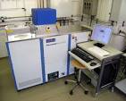
Nanofabrication Equipment
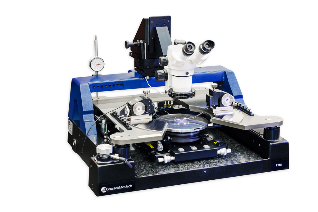 |
Electrical Probe StationCoax – DC parametric test down to pA levels |
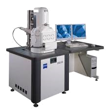 |
Helios NanoLab DualBeam 600 SEMThe Helios NanoLab™ 600 is equipped with an extremely high resolution Elstar™ electron column with a Field Emmission Gun (FEG) electron source. It is capable of <1nm @ 15kV and <2.5nm at 1kV electron beam resolution. The Ga+ ion source can image and machine down to 5nm resolution levels. |
|
|
Hitachi-FSEMThis Hitachi S-4500 field emission scanning electron microscope (FESEM) is capable of producing high-resolution images between 20 and 500k. The system is capable of accelerating voltages between 0.5-30 kV. With precision setup of the aperture and beam it is capable of capturing images with resolution of ~5 nm. The system can accommodate samples up to 2" in diameter on its manual three-dimension sample stage with tilt capability from 0° to 45°. Active image capture and analysis software provided by the Revolution 1.6 software allows analytical data and storage. The system is also equipped with an X-ray Energy Dispersive Spectroscopy |
 |
Laurell SpinnerLaurell Spinner |
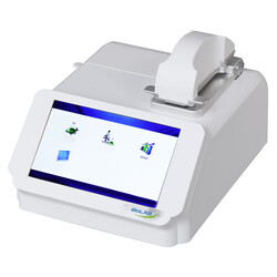 |
Nanospec SpectrophotometerNano Spectrophotometer BSNA-101 |
 |
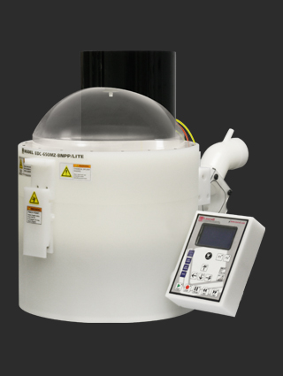
Oxford Plasma Lab SystemThe Oxford system is a load-locked inductively coupled plasma etch tool that uses RF (600 watts 13.56MHz) for the RIE water-cooled electrode and 1.2 kW, 2 MHZ on the ICP driven electrode. The system currently uses Chlorine and Boron tri-chloride gases. |
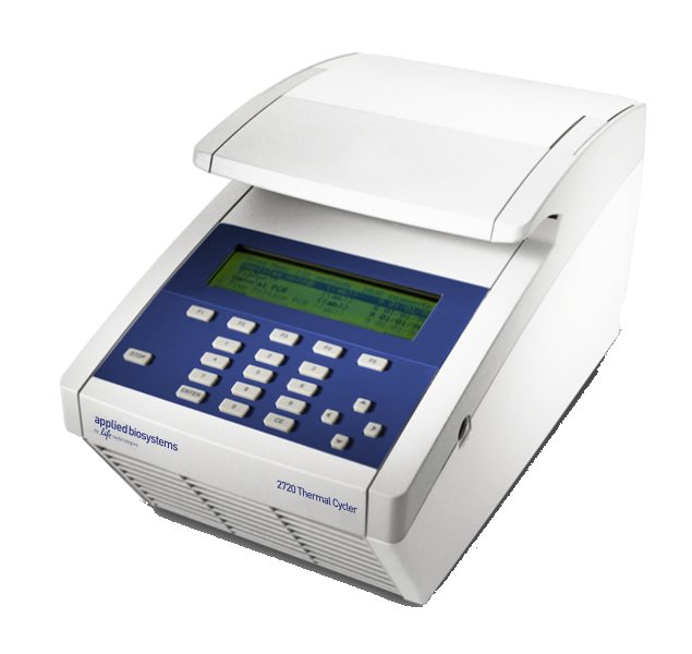 |
Perkin Elmer 2400 |
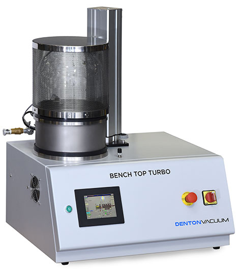 |
Thermal EvaporaterThermal Evaporater |
 |
Vistec EBPG5200The Vistec EBPG5200 is a high-end, state-of-the-art electron beam lithography system that can write to less than 8 nm in size on full 200 nm wafers or small sample pieces. The system uses a high current density thermal field emission gun for operation at 20, 50, and 100kV accelerating voltages. Rapid exposure is possible with up to 50 MHz write speeds and a 20-bit pattern generator. The system incorporates breakthroughs in enhanced resolution, noise reduction, and beam stability for the ultimate in nano-lithography. |
Service Order
MaskThe GCA Mann3600F pattern generator is capable of producing standard 5" x 5" (0.090" thick) or standard 4" x 4" (0.060" thick) chrome mask plates for use in optical lithography. The system is capable of creating mask features to as small as 2 um in size. The masks are originally designed in the L-Edit CAD system and then converted into a format that can be manipulated into data read by the pattern generator. |
Time Clock
 |
Clean Room Access |
This facility has not published any News. Please check back.
Quick Quotes have not been configured. Please check back soon (Code 001, Code 002)
, please enter that email address here.")